
Fiber Optic Connectors & Assemblies
Fiber Array Unit (FAU) Testing Solutions (New)(New)
Polarization-Maintaining Fiber Connectivity Components (New)(New)
Fiber Array (FA) Spot Alignment and Coupling Inspection System
SN-MT Connector Inspection Solutions for Manufacturing
MMC Connector Cleaning and Inspection Solutions for Manufacturing
MPO Connector Inspection Solutions
Automated Cleaning and Inspection for High-Speed Optical Transceivers
1.6T/800G Single-core Optical Module Intelligent Cleaning and Inspection Solution
1.6T/800G LC Optical Module Testing Scheme
Optical Port Cleaning and Inspection for Active Optical Devices
High-Speed Coherent Optical Transceiver Testing
Active Optical Cable (AOC) Testing Solutions
Linear Pluggable Optics (LPO) Testing
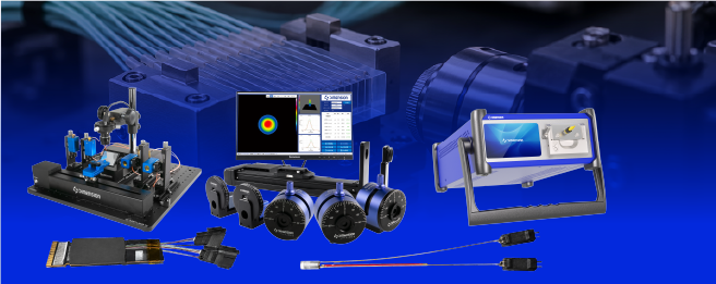
Packaged PIC Testing Solutions
The PIC package integrates the bare chip, fiber array, optical interface and electrical connection into a usable device. After the packaging, tests are required to confirm the transmission performance and identify the effects caused by coupling offset, curing stress, reflection and temperature changes. Dimension Technology builds a testing process for packaging process verification and finished product inspection by focusing on WST scanning, multi-channel power collection and OFDR optical path diagnosis, combined with coupling automation, wavelength and spectrum analysis, and photoelectric control.
Applicable to the tested component
Suitable for PIC packaging devices that have already assembled fiber arrays, tail fibers, lens interfaces or accessible optical windows. Passive packaging chips mainly focus on transmission spectrum, crosstalk and reflection; when containing modulators, detectors or laser units, corresponding electrical, light source and high-speed testing configurations are also provided.

Test Focus
Distinguish the contributions of the chip body, fiber array coupling, and external connection. Comparisons before and after packaging should try to maintain consistency in wavelength, polarization, bias, and reference conditions; after changing the input and output interfaces, the reference plane needs to be reconfirmed to avoid mistakenly interpreting the test connection differences as packaging deterioration.
Scheme Introduction
Monitoring of coupling assembly and curing process
Coupling probe, fiber array fixture, multi-axis positioning table and power feedback
For unfixed fiber arrays, lenses or exposed optical ports, use multi-channel power feedback to perform light search and alignment; simultaneously observe key channels to prevent single channel being optimal while others deviate. For fixed packaged products, use matching fixtures for measurement without repeating internal coupling actions.
Record power changes during dispensing, curing and release fixture stages to form pre- and post-assembly comparison data. Configure curing process and platform movement according to product structure and material requirements.
Multi-port spectral transmission and crosstalk testing
WST wavelength scanning system, TopLight TLS and multi-channel OPM
Measure the transmission spectra, insertion loss, passband position and port isolation of each port, check if the optical path after packaging meets the design. Matrix or multi-channel devices are covered item by item according to port mapping, and the crosstalk results retain the excitation port, observation port and reference power.
Fix TE or TM input according to chip design, or conduct PDL measurement under an appropriate device model. Associate temperature and bias during scanning, distinguish coupling changes, thermal drift and chip tuning.
Photoelectric function and working point verification
SMU drive control, temperature control and optical power acquisition
For modulators, detectors and thermal tuning units, measure the static transmission and bias relationship, dark current, photocurrent and tuning curve, and confirm the packaging electrical connection and working point. When high-speed performance is required, configure matching electrical interface fixtures, biasers, network analysis or error code and oscilloscope measurement links.
Response rate and receiving power use the agreed packaging input reference plane; system link loss and chip intrinsic parameters are recorded separately.
Packaging optical path reflection and fault location
OFDR and return loss test configuration
Total return loss test evaluates external port reflection, OFDR is used for reflection distribution analysis of passive paths, assisting in distinguishing connectors, fiber tails and chip coupling interfaces. Branch paths, non-reciprocal devices or excessive reflection may affect interpretation, it should be combined with device structure verification; paths with different media are explained by segment group refractive indices, cannot be directly applied to a single fiber distance.
Wavelength and spectrum of active packaging devices
Wavelength meter, spectrometer, laser drive and temperature control
For packaged PICs containing laser units, measure the laser wavelength, temperature or current-induced drift, and analyze the spectral mode, side mode and multi-wavelength output. The wavelength meter and spectrometer undertake corresponding measurement tasks respectively; for passive packaged PICs without self-luminous function, preferentially use wavelength-sweep transmission to characterize, no need to configure independent emission spectrum test.

Environmental stability and automated re-testing
Temperature control fixtures or environmental chambers automatically switch and test software
Perform re-testing for temperature maintenance, temperature variation or aging stages according to the verification plan, and correlate power, spectrum, bias and reflection changes. The software archives results by product number, packaging batch, port and process stage; automatic loading and unloading, scanning and electrical connection are integrated according to the production line structure; optical switches are configured only when channel organization is truly necessary.

Advantages of the plan
Pay attention to both performance and the packaging process.
Link the data from the coupling, curing and temperature stages to the same device, making it easier to identify the source of loss changes.
Add supplementary reflection distribution diagnosis.
Combine total return loss with OFDR on applicable paths to increase the basis for observing the internal connection status of the package.
Be compatible with passive and active configurations.
Select spectral, electrical and high-speed test modules based on whether the package contains lasers, modulators and detectors.
Related products and system configuration
Instrument or system | Main purposes and applicable conditions |
TopLight TLS and WST | Transmission spectrum, loss and port isolation tests after packaging |
PPC and Multi-channel OPM | Polarization condition control, multi-port acquisition and coupled feedback |
OFDR and Insertion Loss Tester | Reflection distribution diagnosis and external port total return loss test |
Coupling probe array fixture and multi-axis platform | Monitoring of alignment and curing process for unfixed optical interfaces |
SMU Drive and Temperature Control Configuration | Biasing of active devices, electrical functions and tuning characterization |
Wavelength meter and spectrometer | Laser unit device-based wavelength drift and spectral analysis |
High-speed photoelectric test link | Verify the frequency response and high-speed transmission/reception performance based on the device functions |
Environmental Verification and Automation Platform | Temperature variation re-measurement, loading and unloading, scanning and data traceability |
Select the necessary items based on the function of the tested component. The band, interface, bandwidth, accuracy and automation cycle should be confirmed according to the requirements of the project. The accompanying photoelectric probe, high-speed instrument and environmental equipment can be integrated according to the system requirements.
Easily access services and support from Dimension
Want help or have questions?