
Fiber Optic Connectors & Assemblies
Fiber Array Unit (FAU) Testing Solutions (New)(New)
Polarization-Maintaining Fiber Connectivity Components (New)(New)
Fiber Array (FA) Spot Alignment and Coupling Inspection System
SN-MT Connector Inspection Solutions for Manufacturing
MMC Connector Cleaning and Inspection Solutions for Manufacturing
MPO Connector Inspection Solutions
Automated Cleaning and Inspection for High-Speed Optical Transceivers
1.6T/800G Single-core Optical Module Intelligent Cleaning and Inspection Solution
1.6T/800G LC Optical Module Testing Scheme
Optical Port Cleaning and Inspection for Active Optical Devices
High-Speed Coherent Optical Transceiver Testing
Active Optical Cable (AOC) Testing Solutions
Linear Pluggable Optics (LPO) Testing
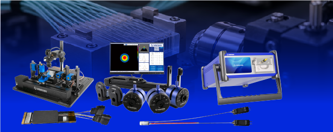
PIC Wafer and Die Testing Solutions
Dimension Technology is based on fiber coupling probes, multi-axis positioning, WST wavelength scanning and measurement, and covers testing requirements for passive optical paths and active units.
Applicable to the tested component
Applicable to wafers with grating coupling interface, wafer structures with accessible edge coupling interface, and cut PIC bare chips. Covers waveguides, beam splitters, multiplexers, filters, as well as chips with integrated modulators, detectors or laser units; the test items are selected according to the actual functions.
Test Focus
Surface coupling and edge coupling are respectively designed with probes, incident angles and motion trajectories. Wafer-level edge coupling requires accessible etched trenches or other test structures; ordinary uncut wafers cannot be directly tested in the bare chip end face manner. During the test, the coupling status is also recorded simultaneously to avoid misjudging the positioning drift as a change in chip performance.
Solution Introduction
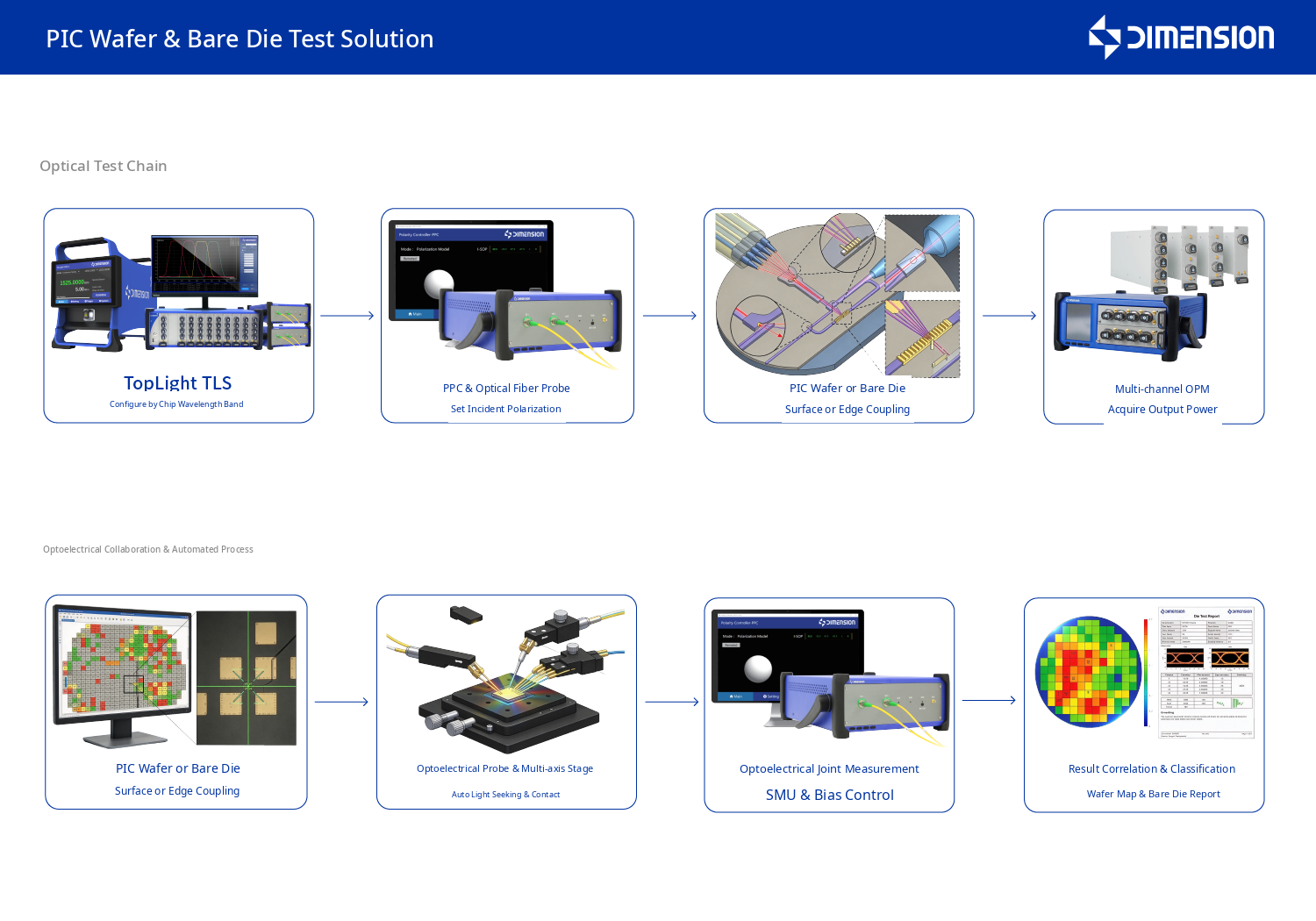
Optical Fiber Coupling Probe and Automatic Light Detection
Optical Fiber Probe or Optical Fiber Array Probe Multi-axis Positioning Table and Vision System
For grating couplers or edge couplers, corresponding probes, fixtures, and motion modes are configured. Input and output alignment is achieved through visual coarse positioning, light power feedback fine adjustment, and pose retention, and probe collision prevention and safe return positions are set. Multi-port chips are configured with single-fiber or array probes according to the channel arrangement.
Wafer testing is carried out point-by-point according to the wafer layout. Bare chip testing uses carrier fixtures and reference marks. The repeatability after re-exposure of light needs to be verified, and the results of position, incident angle, polarization and reference structure should be recorded.
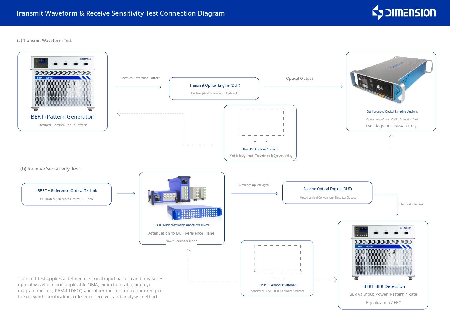
Spectral transmission and polarization response testing
WST wavelength scanning system TopLight TLS PPC and multi-channel OPM
Scan the wavelengths and simultaneously collect each output to obtain transmission spectra, insertion loss, passband, central wavelength, and channel isolation, etc. For polarization-sensitive structures, priority should be given to characterizing under the specified TE or TM input conditions; only when there are appropriate dual-polarization access and model conditions, should the PDL method be used for evaluation.
Perform normalization using the same wafer reference waveguide, reference coupler, or verified test structure. If coupling loss deembedding has not been completed, the link loss including input and output coupling should be reported, and it cannot be directly regarded as the intrinsic loss of the waveguide.
Optoelectronic joint parameter testing
Electroprobe SMU optical power measurement and bias control
Measure dark current, photoelectric current and responsivity of the detector, and measure transmission curves, operating points and static extinction characteristics of the modulator under bias voltage; when equipped with a thermal tuning unit, correlate heating power with spectral drift. Responsivity is calculated based on the actual incident power on the chip reference plane.
When frequency response or high-speed modulation verification is required, add RF probe, biaser, vector network analyzer or high-speed transceiver test link, and complete the corresponding calibration.
Diagnosis and Automated Testing
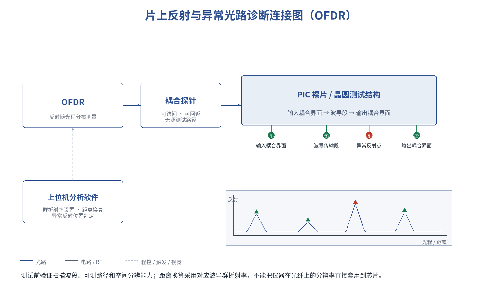
On-chip Reflection and Abnormal Optical Path Diagnosis
OFDR and Matching Coupling Probe
Analyze the distribution of reflection along the optical path on an accessible and returnable passive test path to assist in identifying the input-output coupling interface, waveguide endpoints, or abnormal reflections before packaging. Verify the scanning wavelength range, measurable path, and spatial resolution before testing, using the corresponding waveguide group refractive index for distance conversion; do not directly apply the instrument's resolution on the optical fiber to the chip.
Wavelength and spectrum testing of integrated light sources
Wavelength meter, spectrometer and laser-driven temperature control
Only configured for active bare chips with laser units or detectable optical ports. The wavelength meter is used for laser wavelength and drift measurement, while the spectrometer is used for mode, spectral line distribution and edge-mode suppression ratio analysis; synchronous recording of driving current, temperature and power. Narrow linewidth testing requires an alternative method, and the laser linewidth cannot be directly claimed using conventional spectral resolution.
Wafer scanning and die grading
Automatic probe station, test software and data management
Map the wafer number, Die coordinates, device units and ports to the test recipe, and perform automatic light search, biasing, wavelength scanning and result determination. Trigger re-testing based on reference structure and stability check results, and form wafer distribution map, abnormal list and die grading records.

Scheme Advantages
Integrating coupling and measurement into the same process
Linking optical position, polarization and electrical bias for easier analysis of chip differences and test fluctuations.
Supporting pre-packaging screening
Linking spectra, electrical and specified diagnostic results to the bare chip to reduce defective chips flowing into subsequent assembly.
Configuring instruments according to chip functions
Prioritizing scanning and power measurement for passive structures, and adding electrical, high-speed or light source characterization for active structures.
Related products and system configuration
Instrument or system | Main purposes and applicable conditions |
TopLight TLS and WST | Wavelength scanning, transmission spectrum and multi-port optical parameters |
PPC and Multi-channel OPM | Control the input polarization and collect power feedback |
Coupling probe and multi-axis positioning platform | Surface or edge coupling, automatic light seeking and position retention |
Electroprobe SMU and temperature control console | Analog unit DC parameters, biasing and temperature control |
OFDR | Reflection distribution diagnosis applicable to passive paths |
Wavelength meter and spectrometer | Characterization of wavelength and spectrum of chips with laser units |
RF probe and high-speed measurement link | Carry out electro-optic frequency response and high-speed performance verification as needed |
Wafer or bare chip automation software | Coordinate scheduling, formula execution, retesting and grading |
Select the necessary items based on the function of the tested component. The band, interface, bandwidth, accuracy and automation cycle should be confirmed according to the requirements of the project. The accompanying photoelectric probe, high-speed instrument and environmental equipment can be integrated according to the system requirements.
Easily access services and support from Dimension
Want help or have questions?