- Home
-
Solutions
High-Speed Optical Module R&D and Manufacturing Optical Passive Components R&D and Manufacturing Optical Connector R&D and Manufacturing Optical Communication Device Production and Manufacturing AI and Data Center Optical Network Operation & Maintenance Optical Communication Automation and Intelligent Testing Enterprise Network and Data Center Fiber Optic Sensing Testing and Application Academic and Research InstitutionsHigh-Speed Optical Module R&D and Manufacturing1.6T/800G LC Optical Module Testing Solution 1.6T/800G MPO Optical Module Testing Solution 1.6T/800G High-Speed Optical Module Testing FA/JUMPER Test Solution High speed optical module micro connection Active chip production and manufacturing Research and manufacturing of CPO/NPO co packaging technology PIC Testing and Packaging for Silicon Photonics Cleaning and detection of optical active device ports Automated production and manufacturing solutionsOptical Passive Components R&D and ManufacturingFA/JUMPER Test Solution High speed optical module micro connection Device Development and Testing for NPO CPO Optical Interconnects DWDM AWG WSS Automated Production and Testing MPO connector detection solution Production testing of splitter, ring-shaped isolator, and optical switch Polarization maintaining device testing Passive Component Environmental Reliability Testing Automated production and manufacturing solutions Optical fiber and cable testingOptical Connector R&D and ManufacturingTesting Solutions For SN/CSConnector Production and Application Testing Solutions for SN-MTConnector Production and Application MDC Production Inspection Solution The inspecting solutions of MMC connectors FA/JUMPER Test Solution MPO connector detection solution The inspecting Solution of single/duplex connectors Inspection and cleaning of connector end faces Insertion Loss and Return Loss Performance Testing End-face geometry inspectionOptical Communication Device Production and ManufacturingFA/JUMPER Test Solution 1.6T/800G High-Speed Optical Module Testing Active chip production and manufacturing Research and manufacturing of CPO/NPO co packaging technology PIC Testing and Packaging for Silicon Photonics Cleaning and detection of optical active device ports Automated production and manufacturing solutions High speed optical module micro connection DWDM AWG WSS Automated Production and Testing MPO connector detection solution
-
Products
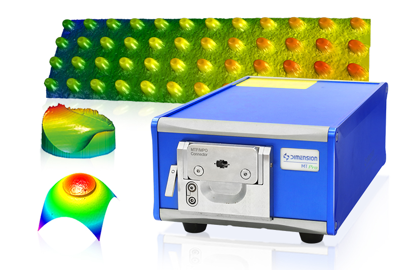
Optical Network Operations Testing Optical Passive Components Transceiver Research and Manufacturing Fiber Connector Manufacturing Automation Data Center Fiber Sensing & Optics
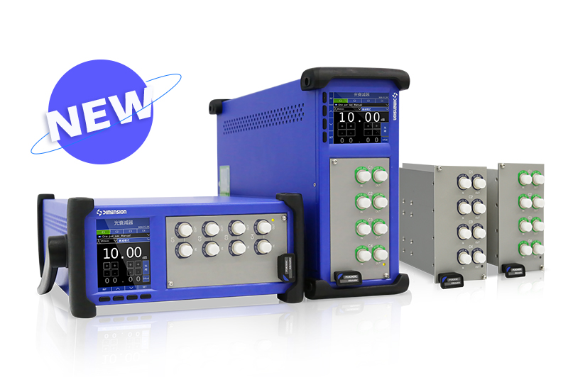
Latest Releases

Testing Optical Passive Components
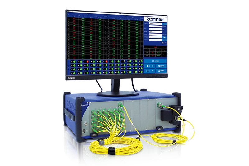
Latest Releases
Transceiver Research and Manufacturing
Latest Releases
Latest Releases
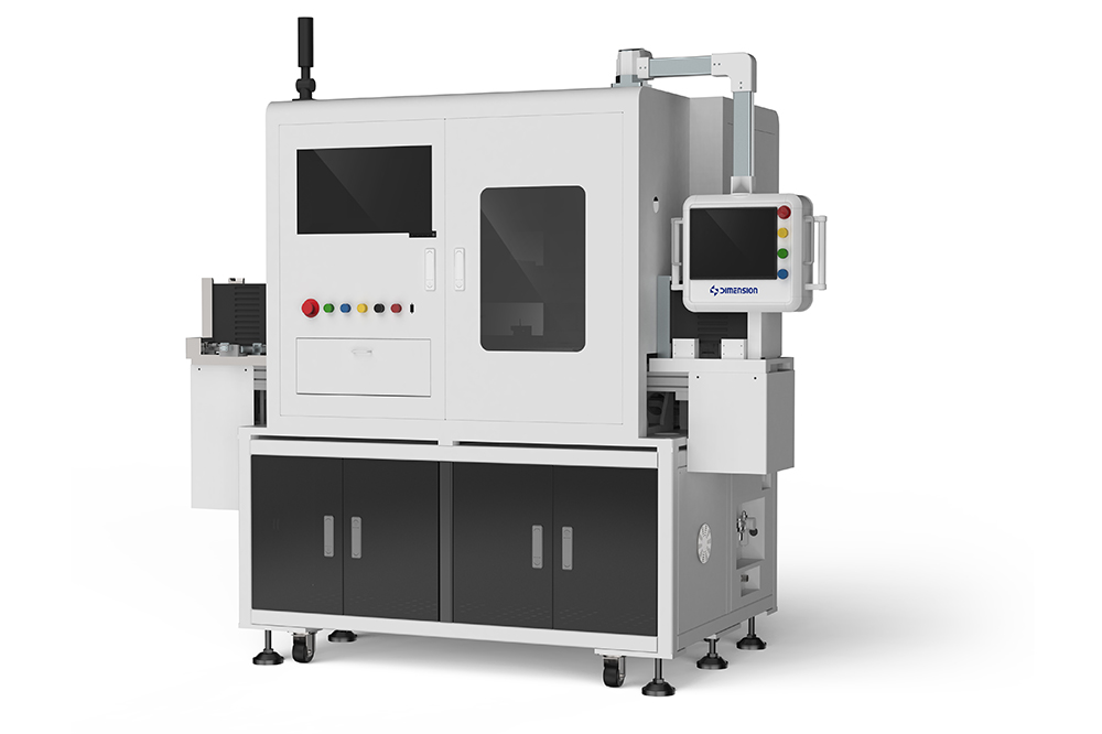
Automated Production and Manufacturing System
800G and 400G module cleaning and visual inspection system Auto CVI (Cleaning and Visual Inspection) System for LC/SC Optical Modules Automatic cleaning and detection system for optical components TOSA and BOSA automatic cleaning and detection systems MT connector automatic cleaning and detection system Tailored solutions for non-standard automated productionLatest Releases
Optical Fiber End Face Inspection and Cleaning
EasyGet WiFi Wireless Fiber Endface Microscope AutoGet Wifi Intelligent Fiber Endface Microscope EasyCleaner Optical fiber connector cleaner EasyGet2 Portable Fiber Endface Microscope EASYSTICK Fiber Cleaning Cotton Stick OPTIPOP Optical Connector Cleaner NEOCLEAN™ SERIES Optical Connector Cleaner Lineup New Fiber Elbow AdapterLatest Releases
800G and 400G module cleaning and visual inspection system Auto CVI (Cleaning and Visual Inspection) System for LC/SC Optical Modules Automatic cleaning and detection system for optical components TOSA and BOSA automatic cleaning and detection systems MT connector automatic cleaning and detection system Tailored solutions for non-standard automated productionFast Check MT Fully Fiber Endface Inspector EasyCheck V2 Digital Fiber Endface Inspector EasyCheck Dual Magnification Fiber Endface Inspector AutoCheck Integrated Fiber Endface Inspector SmartCheck Intelligent Fiber Endface Inspector Fastcheck PRO Fully Automatic Fiber Endface Inspector EASYCHECK AF Autofocus Fiber Endface Inspector FA-1 Fiber Array Endface Inspector - Services
- About Us